


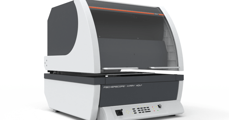
Helmut Fischer FISCHERSCOPE X-RAY XDV-µ series – microstructure measurement with polycapillary optics
Applications
For the electronics and semiconductor industry – for measuring conductor tracks, contacts, lead frames, SMD components, thin wires and complex multilayer systems, and the phosphorus content of electroless nickel layers under gold and palladium (ENIG/ENEPIG). Fischer is the only XRF manufacturer with its own production of polycapillary optics.
Key features
- “Ultra” microfocus tube and polycapillary optics – high intensity in the smallest spots
- DPP+ – up to 50 % higher performance compared with DPP
- Programmable measurements based on pattern recognition; fully automatable with one click
- Video system with threefold optical zoom
- LD: largest measuring distance in its class of 12 mm, XY stage with ≤ 2 µm positioning accuracy
- WAFER: vacuum stage for wafers of all standard formats 150–300 mm
Models
XDV-µ (spot approx. Ø 10 or 17 µm, samples up to 135 mm); XDV-µ LD (spot approx. Ø 35 µm, distance 12 mm, up to 135 mm); XDV-µ WAFER (wafers 6–12 in., sample up to 5 mm). Polycapillary options: 10 µm without halo, 20 µm without halo, 20 µm with halo
Technical data
- X-ray tube: “Ultra” microfocus, tungsten anode (molybdenum optional)
- Detector: SDD 20 or 50 mm²
- Measuring spot: XDV-µ approx. Ø 10 / 17 µm; LD approx. Ø 35 µm
- Measuring distance: LD – 12 mm
- Sample height: up to 135 mm (XDV-µ, LD); up to 5 mm (WAFER)
- Filters: interchangeable (WAFER – 4 interchangeable)
- Coatings: < 0.1 µm; Au/Pd < 10 nm (WAFER)
- Software: WinFTM
What we offer
- Selection of the instrument and configuration for your task, together with the manufacturer
- Trial measurements of your samples in the manufacturer’s laboratory
- Training, calibration and service organised through the manufacturer
Technical data according to the manufacturer: helmut-fischer.com, helmut-fischer.com
You might also be interested in
Helmut Fischer FISCHERSCOPE X-RAY XDV-µ SEMI – automated wafer microstructure inspection
For semiconductor manufacturing and packaging (2.5D/3D) – inspection of nanometre-scale under-bump metallisation (UBM), C4 and smaller solder bumps, and lead-free solder caps on copper pillars.
Helmut Fischer FISCHERSCOPE XDV-µ PCB XL – coating inspection of printed circuit boards
For PCB manufacturers and EMS companies inspecting thin final finishes (ENIG, ENEPIG, immersion Ag and Sn) on large boards.