


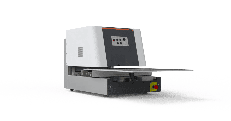
Helmut Fischer FISCHERSCOPE XDV-µ PCB XL – coating inspection of printed circuit boards
Applications
For PCB manufacturers and EMS companies inspecting thin final finishes (ENIG, ENEPIG, immersion Ag and Sn) on large boards. The PCB XL is a benchtop instrument operated in manual, semi-automatic or fully automatic mode and designed for integration into automated lines (Smart Factory). For entry-level tasks – XDLM-PCB, for universal tasks – XDAL-PCB.
Key features
- Largest measuring area in its class – one-time positioning, higher throughput
- Optional vacuum holder for thin and flexible boards
- Stage extension by foot pedal; industrial frame for stability
- Automatic finding of measuring positions by pattern recognition
- Results comply with IPC standards for PCB finishes
- Analysis of Au/Pd coatings ≤ 3 nm or 10 nm
Models
XDV-µ PCB XL (SDD 20/50 mm², W or Mo anode, 10 µm optics, vacuum holder optional); X-RAY XDV-µ PCB (up to 610 × 610 mm, spot 10/17 µm, sample up to 10 mm); X-RAY XDAL-PCB (SDD, spot approx. Ø 0.2 mm, up to 10 mm, stage 610 × 610 mm, extension up to 1200 × 900 mm); X-RAY XDLM-PCB 200/210/220 (proportional counter, spot approx. Ø 0.2 mm, up to 5 mm, 610 × 610 mm, extension 1200 × 900 mm)
Standards
IPC 4552 and IPC 4556 (ENIG, ENEPIG); IPC 4553A (silver); IPC 4554 (tin)
What we offer
- Selection of the instrument and configuration for your task, together with the manufacturer
- Trial measurements of your samples in the manufacturer’s laboratory
- Training, calibration and service organised through the manufacturer
Technical data according to the manufacturer: helmut-fischer.com, helmut-fischer.com
You might also be interested in
Helmut Fischer FISCHERSCOPE X-RAY XDV-µ series – microstructure measurement with polycapillary optics
For the electronics and semiconductor industry – for measuring conductor tracks, contacts, lead frames, SMD components, thin wires and complex multilayer systems, and the phosphorus content of electroless nickel layers under gold and palladium (ENIG/ENEPIG).
Helmut Fischer FISCHERSCOPE X-RAY XDV-µ SEMI – automated wafer microstructure inspection
For semiconductor manufacturing and packaging (2.5D/3D) – inspection of nanometre-scale under-bump metallisation (UBM), C4 and smaller solder bumps, and lead-free solder caps on copper pillars.